


Myth vs Fact: Is India Only Assembling Chips, or Building Real Silicon IP?
The global semiconductor value chain spans three distinct layers:
Design & EDA (IP & Architecture)Fabrication (Foundries/Fabs)ATMP/OSAT (Assembly, Testing, Marking, and Packaging)Here is how public perception compares to industry realities:
❌ Myth 1: "India doesn't design chips; it only builds packaging units.
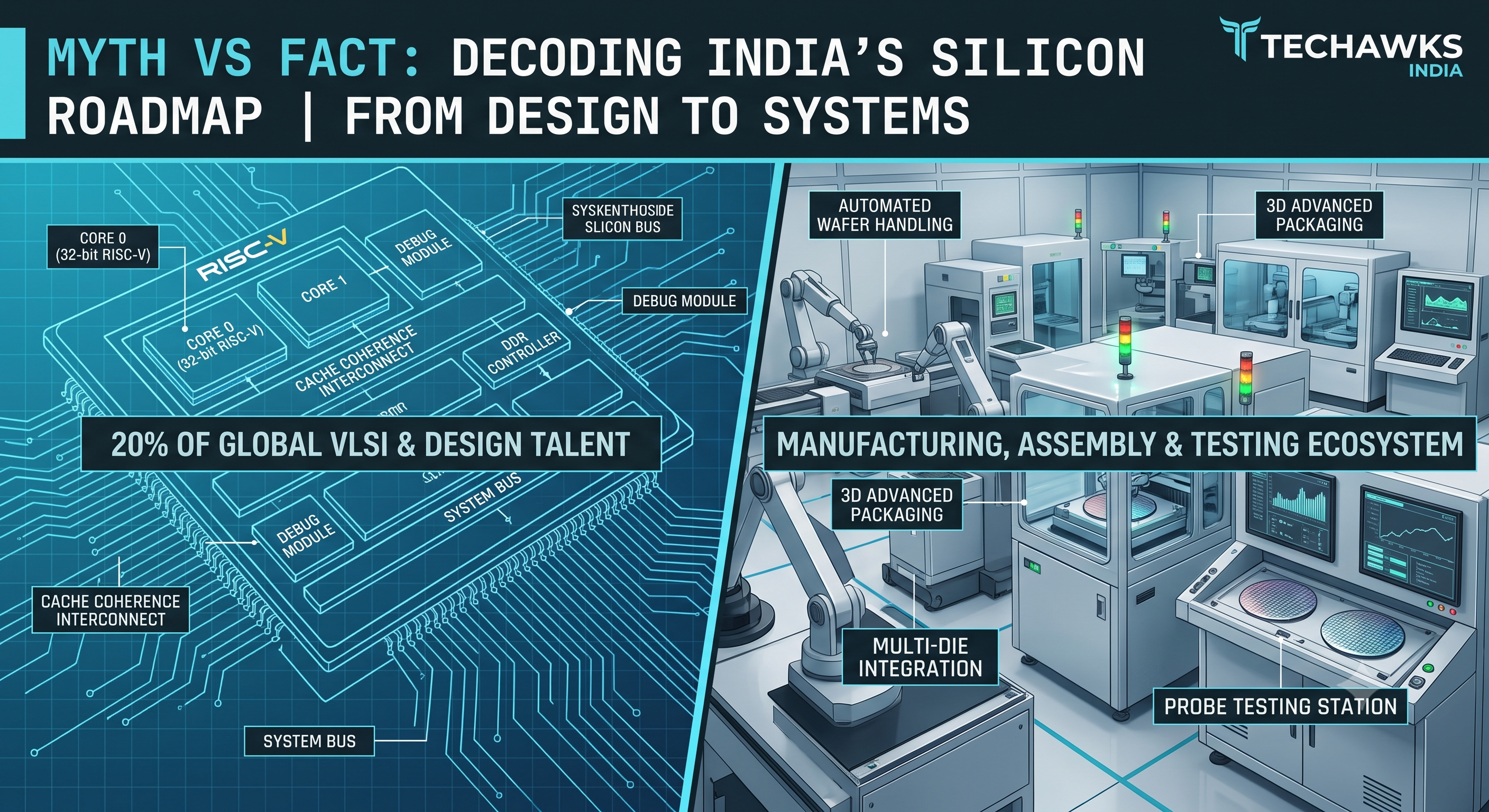
"The Reality: India already houses nearly 20% of the world’s chip design and VLSI workforce. Every major global chipmaker—Intel, Qualcomm, NVIDIA, MediaTek, AMD, and Texas Instruments—runs critical processor architecture, verification, and physical design engines out of Bengaluru, Hyderabad, and Noida. Under the Chips to Startup (C2S) and DLI (Design Linked Incentive) initiatives, over 200 indigenous tape-outs have been completed across Indian institutes and fabless startups down to 12nm nodes. We design the logic; what India historically outsourced was the physical foundry layer.
❌ Myth 2: "Advanced Packaging (ATMP/OSAT) is just low-end screwdriver work.
"The Reality: In the AI accelerator era, monolithic dies have hit thermal and reticle boundaries. Modern computing relies on Heterogeneous Integration and 3D Chiplets (stacking memory like HBM directly on logic dies). High-end ATMP/OSAT is advanced precision engineering requiring cleanrooms, micro-bump bonding, and advanced thermals—not manual board stuffing. Establishing OSAT and compound semiconductor facilities (like those rolling out across Gujarat, Uttar Pradesh, and Odisha) is the prerequisite infrastructure for domestic silicon manufacturing.
❌ Myth 3: "Indian engineers only need to focus on web, app, and cloud layers.
"The Reality: The explosion of Agentic AI, Edge AI, and Robotics means software efficiency is now constrained by compute architecture. Compilers, embedded firmware, kernel drivers, and Electronic Design Automation (EDA) tooling are where the highest-value engineering talent is congregating. If you only write high-level code without grasping hardware acceleration (TPUs, NPUs, RISC-V), your software stack will soon hit a performance ceiling. Why It Matters for Developers & Tech Professionals Silicon sovereignty isn't an abstract geopolitical slogan—it dictates where deep-tech venture capital, R&D labs, and high-paying systems engineering jobs land over the next decade.
Discussion Question
For the engineers and builders in our community: Are you planning to upskill in hardware-adjacent stacks (RISC-V, CUDA, embedded AI, VLSI), or do you see your core focus staying strictly at the application layer? Let's discuss in the comments below! 👇
CTA
Join Techawks India — The premier community for Indian software developers, hardware architects, and tech innovators building the future from India, for the world. 🦅🇮🇳
The global semiconductor value chain spans three distinct layers:
Design & EDA (IP & Architecture)Fabrication (Foundries/Fabs)ATMP/OSAT (Assembly, Testing, Marking, and Packaging)Here is how public perception compares to industry realities:
❌ Myth 1: "India doesn't design chips; it only builds packaging units.
"The Reality: India already houses nearly 20% of the world’s chip design and VLSI workforce. Every major global chipmaker—Intel, Qualcomm, NVIDIA, MediaTek, AMD, and Texas Instruments—runs critical processor architecture, verification, and physical design engines out of Bengaluru, Hyderabad, and Noida. Under the Chips to Startup (C2S) and DLI (Design Linked Incentive) initiatives, over 200 indigenous tape-outs have been completed across Indian institutes and fabless startups down to 12nm nodes. We design the logic; what India historically outsourced was the physical foundry layer.
❌ Myth 2: "Advanced Packaging (ATMP/OSAT) is just low-end screwdriver work.
"The Reality: In the AI accelerator era, monolithic dies have hit thermal and reticle boundaries. Modern computing relies on Heterogeneous Integration and 3D Chiplets (stacking memory like HBM directly on logic dies). High-end ATMP/OSAT is advanced precision engineering requiring cleanrooms, micro-bump bonding, and advanced thermals—not manual board stuffing. Establishing OSAT and compound semiconductor facilities (like those rolling out across Gujarat, Uttar Pradesh, and Odisha) is the prerequisite infrastructure for domestic silicon manufacturing.
❌ Myth 3: "Indian engineers only need to focus on web, app, and cloud layers.
"The Reality: The explosion of Agentic AI, Edge AI, and Robotics means software efficiency is now constrained by compute architecture. Compilers, embedded firmware, kernel drivers, and Electronic Design Automation (EDA) tooling are where the highest-value engineering talent is congregating. If you only write high-level code without grasping hardware acceleration (TPUs, NPUs, RISC-V), your software stack will soon hit a performance ceiling. Why It Matters for Developers & Tech Professionals Silicon sovereignty isn't an abstract geopolitical slogan—it dictates where deep-tech venture capital, R&D labs, and high-paying systems engineering jobs land over the next decade.
Discussion Question
For the engineers and builders in our community: Are you planning to upskill in hardware-adjacent stacks (RISC-V, CUDA, embedded AI, VLSI), or do you see your core focus staying strictly at the application layer? Let's discuss in the comments below! 👇
CTA
Join Techawks India — The premier community for Indian software developers, hardware architects, and tech innovators building the future from India, for the world. 🦅🇮🇳
Myth vs Fact: Is India Only Assembling Chips, or Building Real Silicon IP?
The global semiconductor value chain spans three distinct layers:
Design & EDA (IP & Architecture)Fabrication (Foundries/Fabs)ATMP/OSAT (Assembly, Testing, Marking, and Packaging)Here is how public perception compares to industry realities:
❌ Myth 1: "India doesn't design chips; it only builds packaging units.
"The Reality: India already houses nearly 20% of the world’s chip design and VLSI workforce. Every major global chipmaker—Intel, Qualcomm, NVIDIA, MediaTek, AMD, and Texas Instruments—runs critical processor architecture, verification, and physical design engines out of Bengaluru, Hyderabad, and Noida. Under the Chips to Startup (C2S) and DLI (Design Linked Incentive) initiatives, over 200 indigenous tape-outs have been completed across Indian institutes and fabless startups down to 12nm nodes. We design the logic; what India historically outsourced was the physical foundry layer.
❌ Myth 2: "Advanced Packaging (ATMP/OSAT) is just low-end screwdriver work.
"The Reality: In the AI accelerator era, monolithic dies have hit thermal and reticle boundaries. Modern computing relies on Heterogeneous Integration and 3D Chiplets (stacking memory like HBM directly on logic dies). High-end ATMP/OSAT is advanced precision engineering requiring cleanrooms, micro-bump bonding, and advanced thermals—not manual board stuffing. Establishing OSAT and compound semiconductor facilities (like those rolling out across Gujarat, Uttar Pradesh, and Odisha) is the prerequisite infrastructure for domestic silicon manufacturing.
❌ Myth 3: "Indian engineers only need to focus on web, app, and cloud layers.
"The Reality: The explosion of Agentic AI, Edge AI, and Robotics means software efficiency is now constrained by compute architecture. Compilers, embedded firmware, kernel drivers, and Electronic Design Automation (EDA) tooling are where the highest-value engineering talent is congregating. If you only write high-level code without grasping hardware acceleration (TPUs, NPUs, RISC-V), your software stack will soon hit a performance ceiling. Why It Matters for Developers & Tech Professionals Silicon sovereignty isn't an abstract geopolitical slogan—it dictates where deep-tech venture capital, R&D labs, and high-paying systems engineering jobs land over the next decade.
Discussion Question
For the engineers and builders in our community: Are you planning to upskill in hardware-adjacent stacks (RISC-V, CUDA, embedded AI, VLSI), or do you see your core focus staying strictly at the application layer? Let's discuss in the comments below! 👇
CTA
Join Techawks India — The premier community for Indian software developers, hardware architects, and tech innovators building the future from India, for the world. 🦅🇮🇳

 English
 Arabic
 French
 Spanish
 Portuguese
 Turkish
 Dutch
Dutch
 Italiano
 Russian
 Romaian
 Portuguese (Brazil)
 Greek
Greek